An innovative blend of advanced tech and workplace elements.
SERVICES PROVIDED:
Architecture
Interiors
Structural Engineering
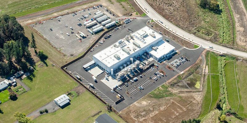
This advanced technology and office building project was designed to drive innovation. Early project and site development was supported by the Hillsboro Economic Council, with the goal of growing high-tech industry and investment. It’s not just a cutting-edge facility, but a significant regional win in the ultra-competitive international semiconductor industry.
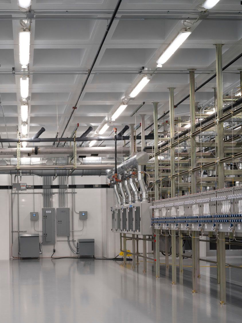
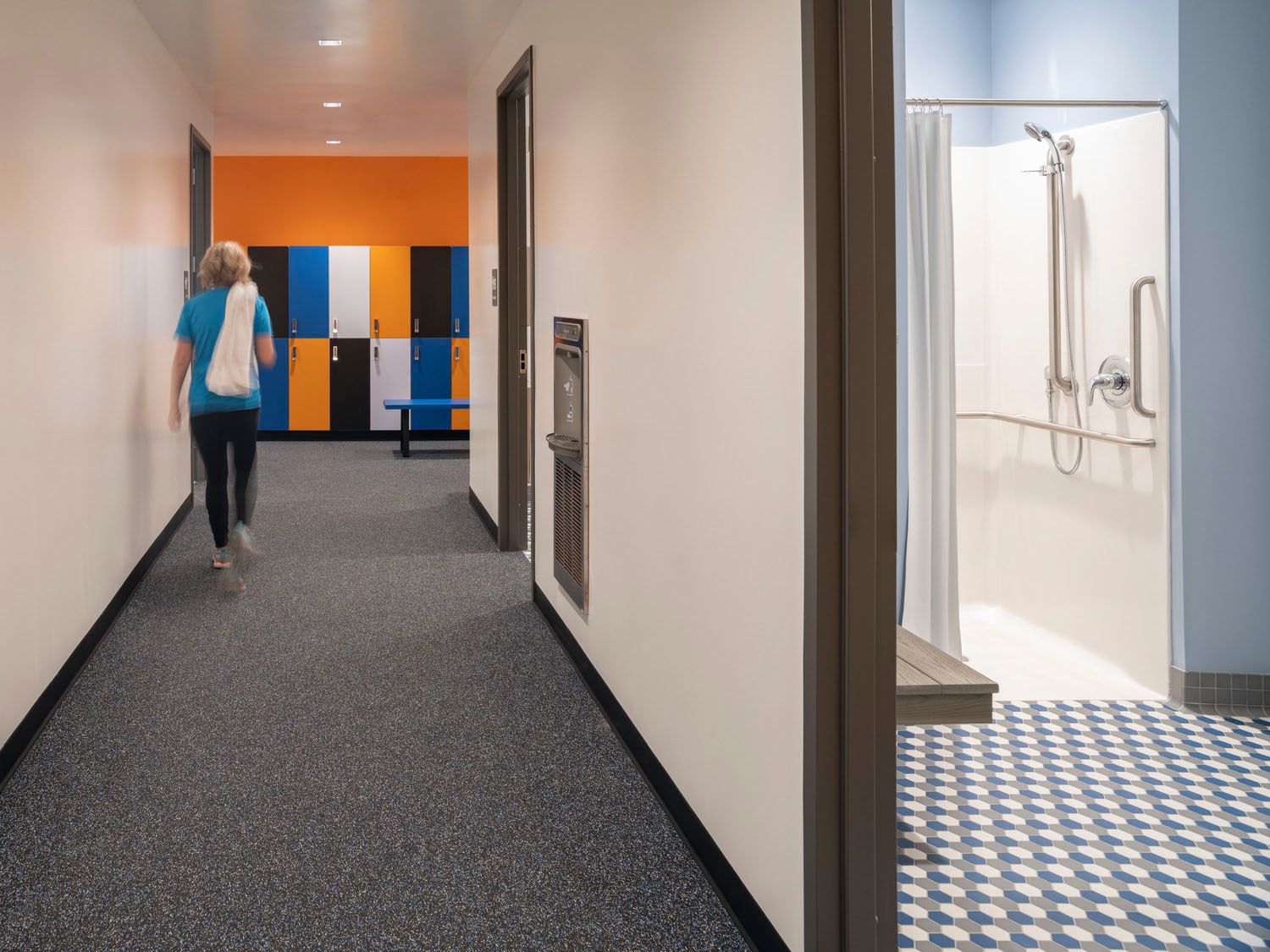
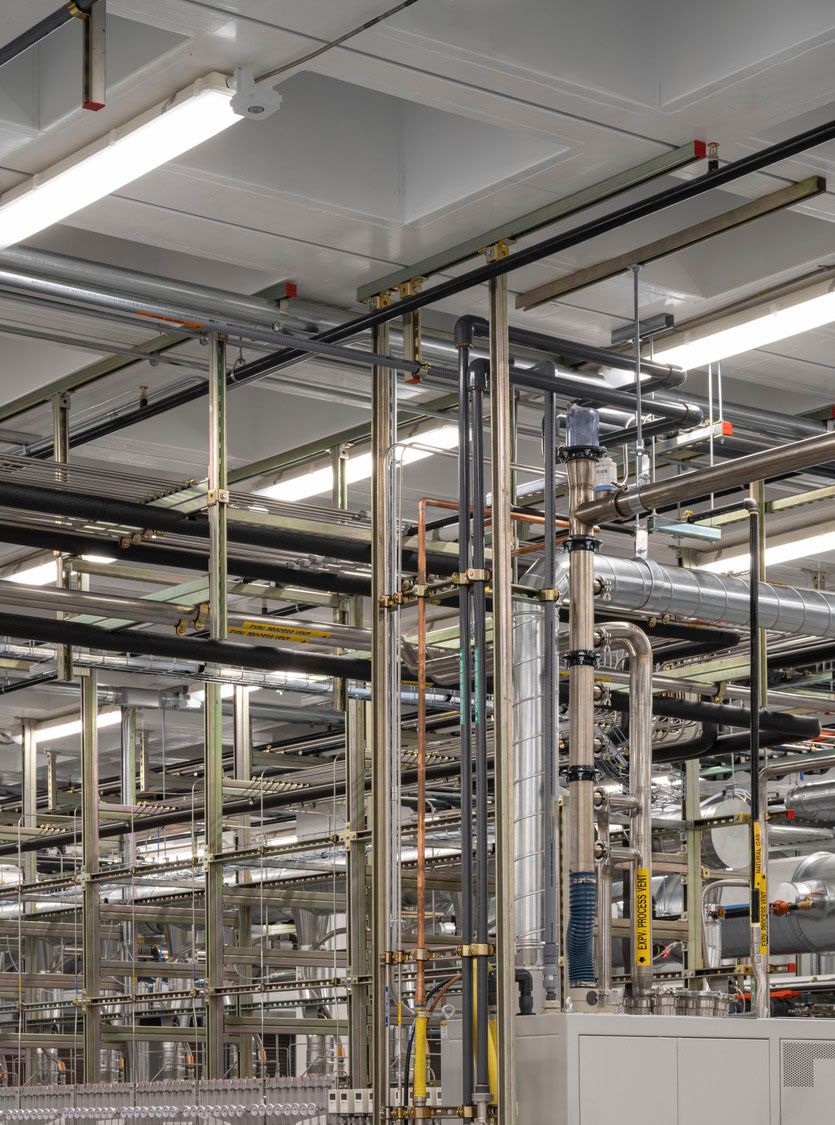
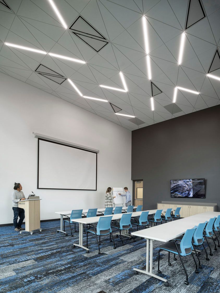
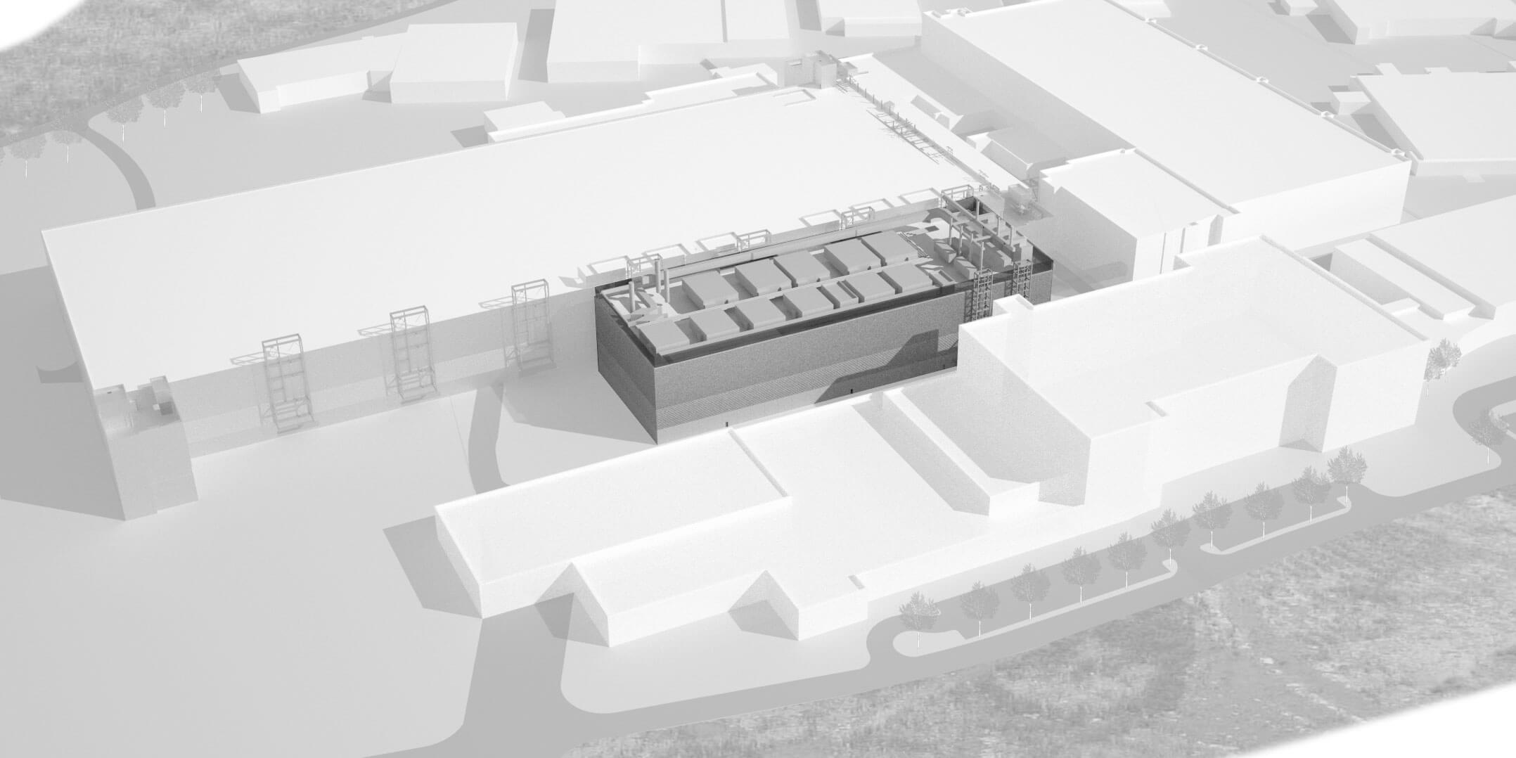
The 218,000 SF project is unique in its blend of office, research and development, and advanced tech elements. The facility includes office space for inter-division collaboration; cleanroom Fab/Subfab for R&D and product demonstration; semiconductor tool layout planning; a microscope lab; training classrooms; mechanical and electrical support rooms; and warehouse space.
DESIGN DRIVERS
The project was designed to attract and retain a highly talented, specialized workforce that will drive innovation in a competitive, complex, and global advanced tech market.
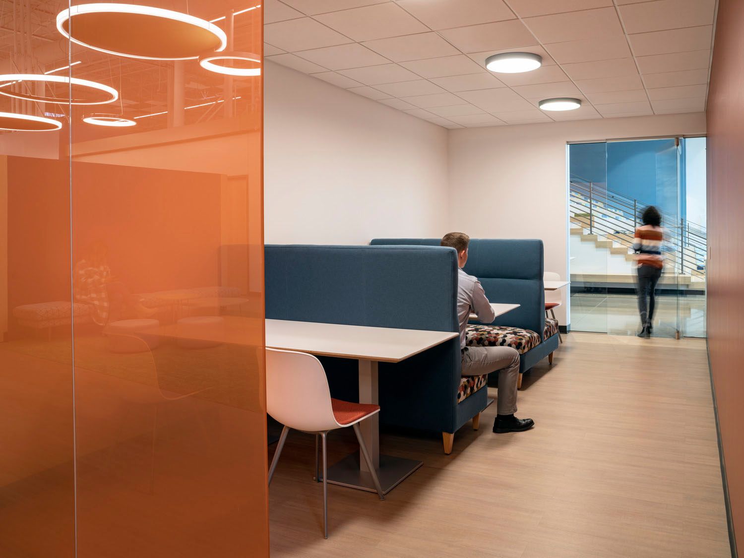
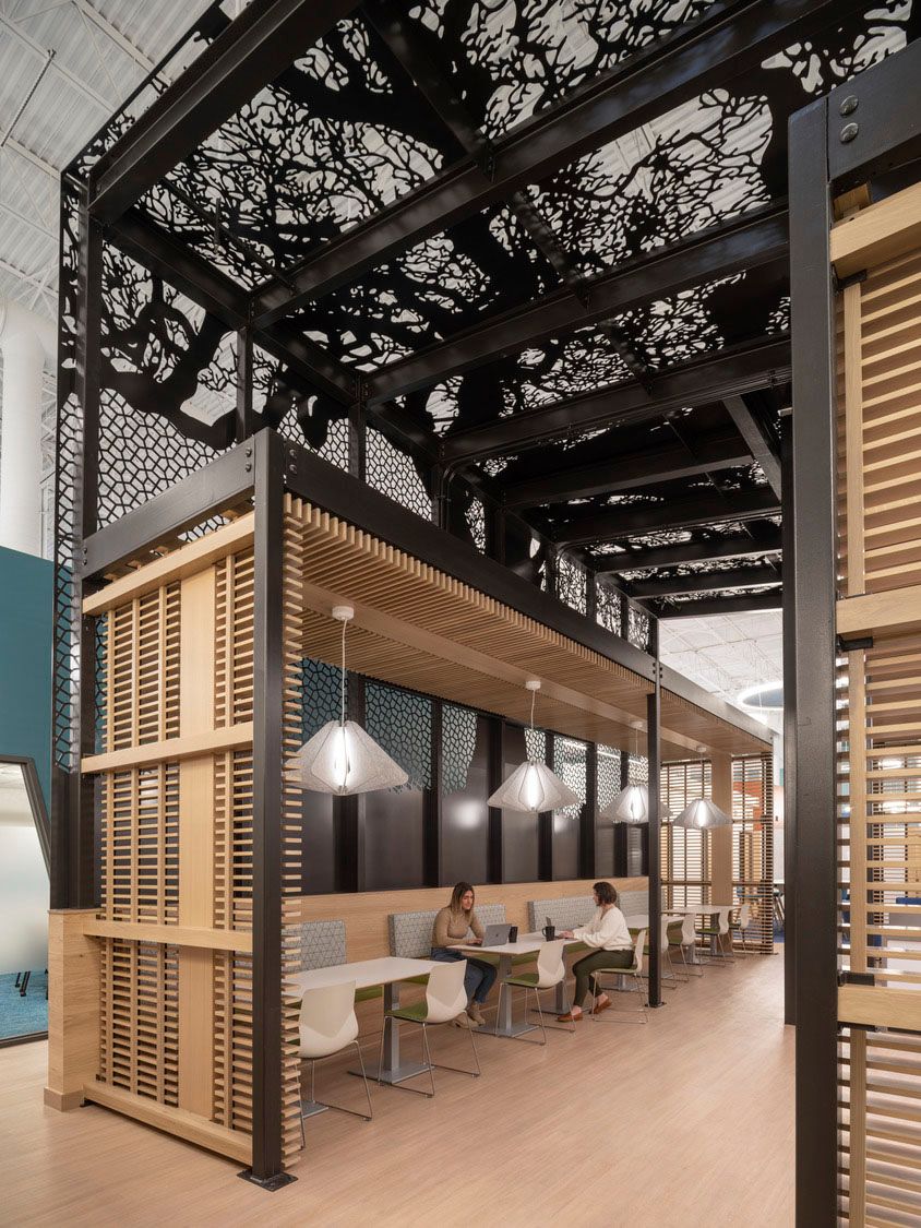
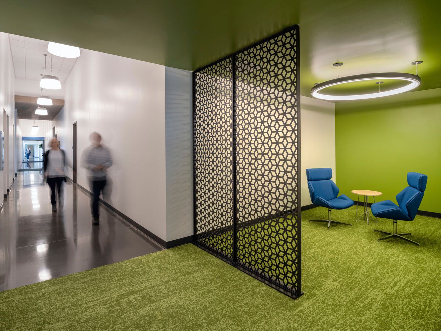
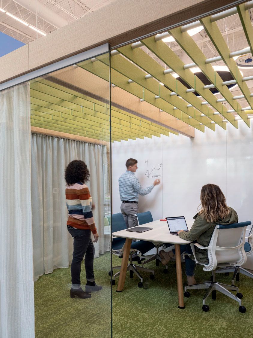
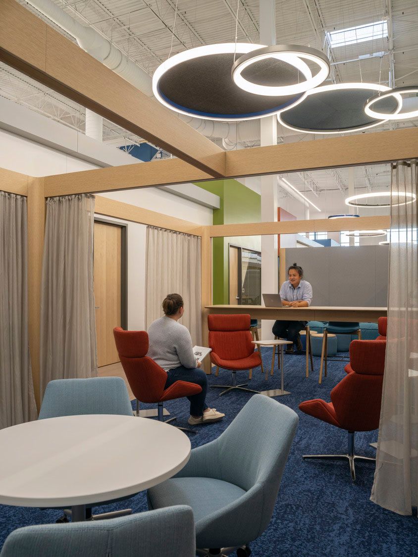
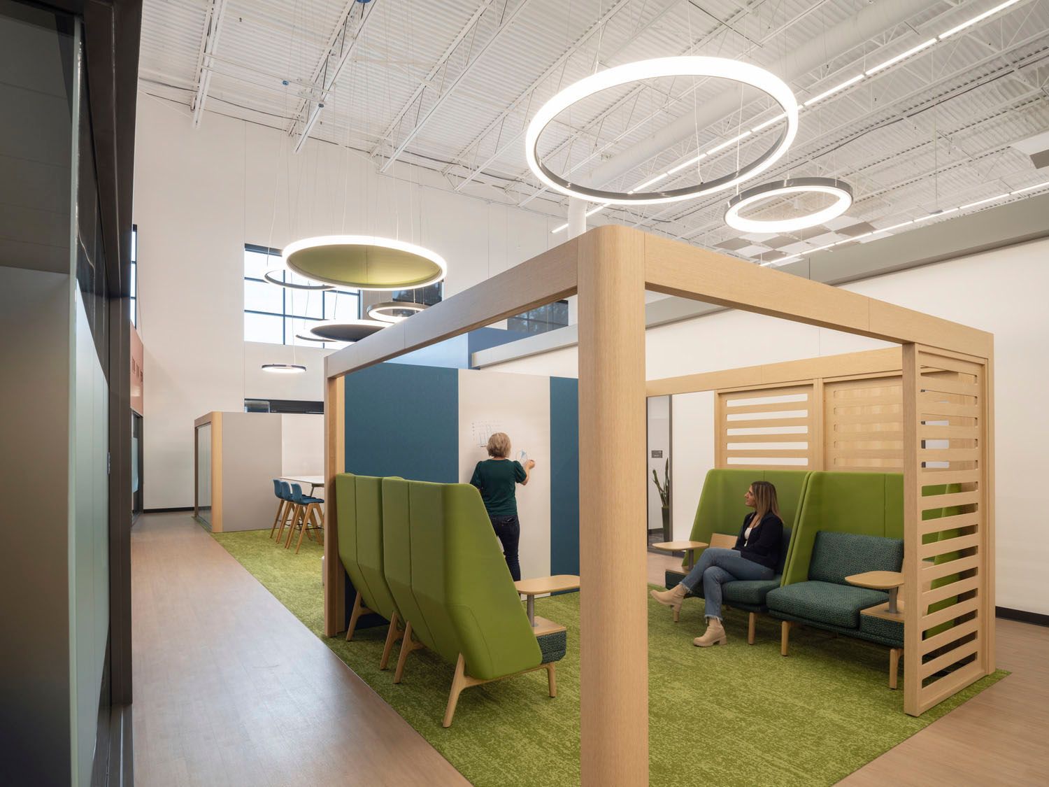
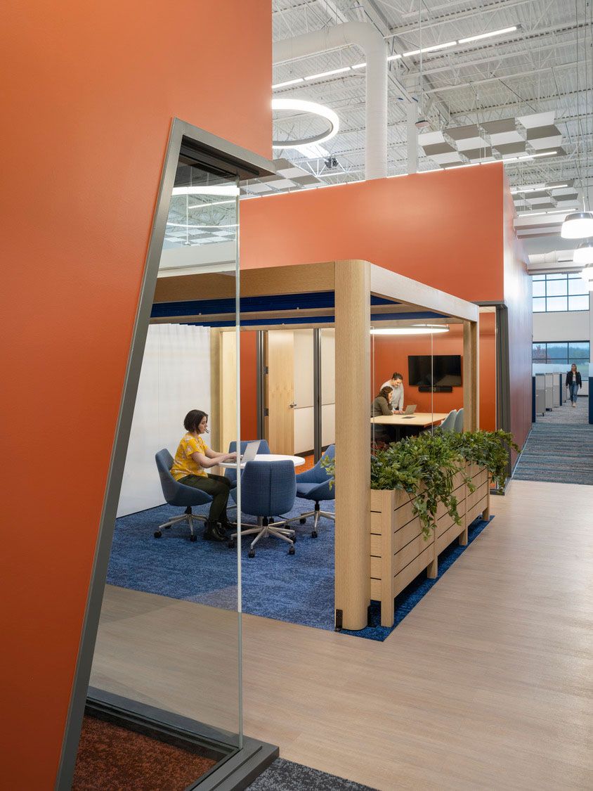
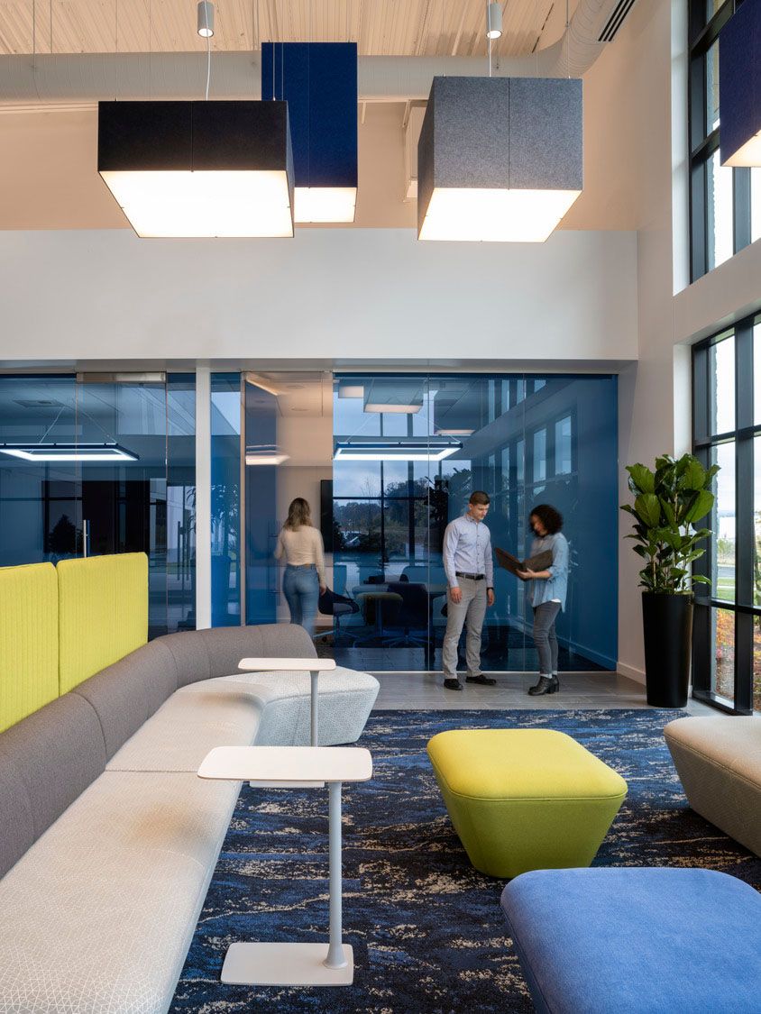
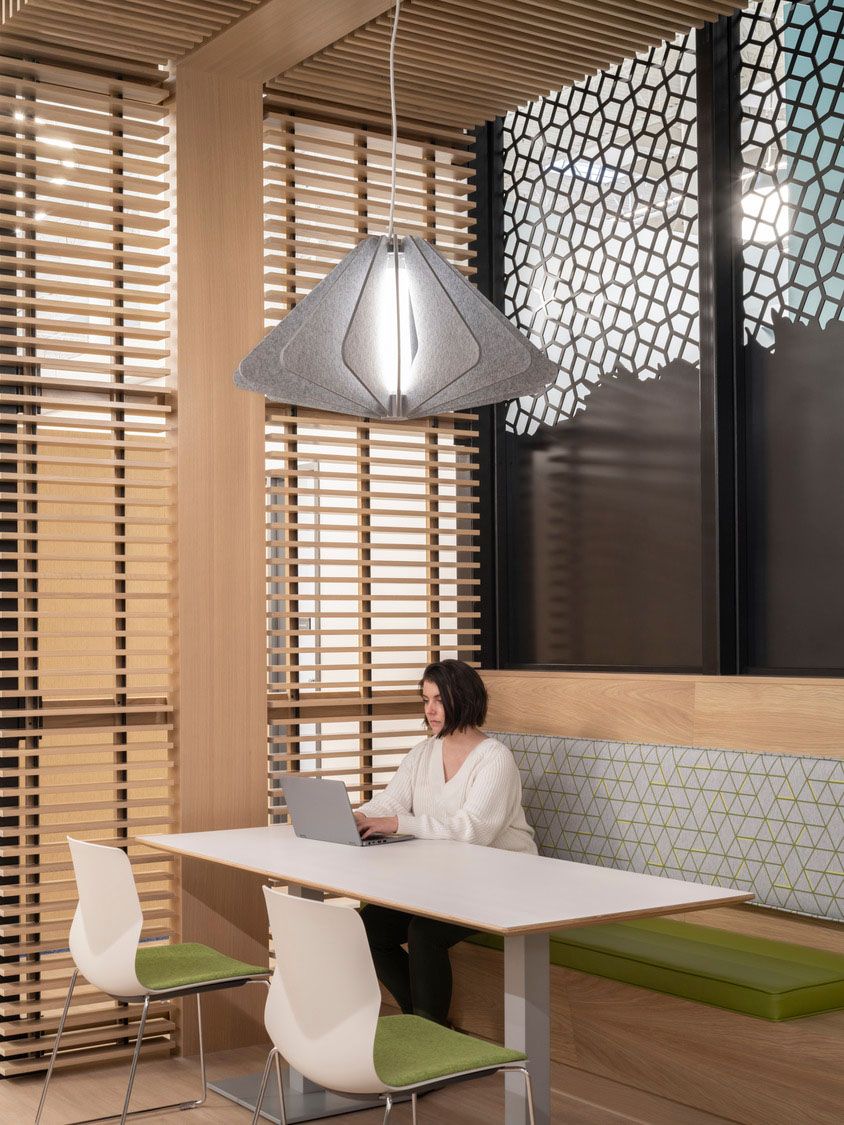
The design creates collaborative neighborhoods organized around a common boulevard that allows for different work style options, and an array of amenities.
The program balances the facility's diverse but intertwined functions, and makes this diversity a foundation for ongoing innovation.
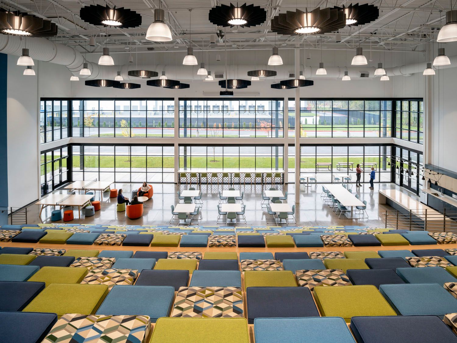
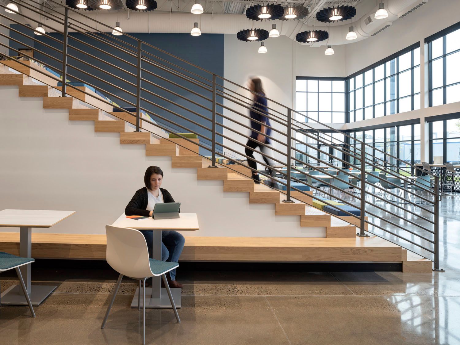
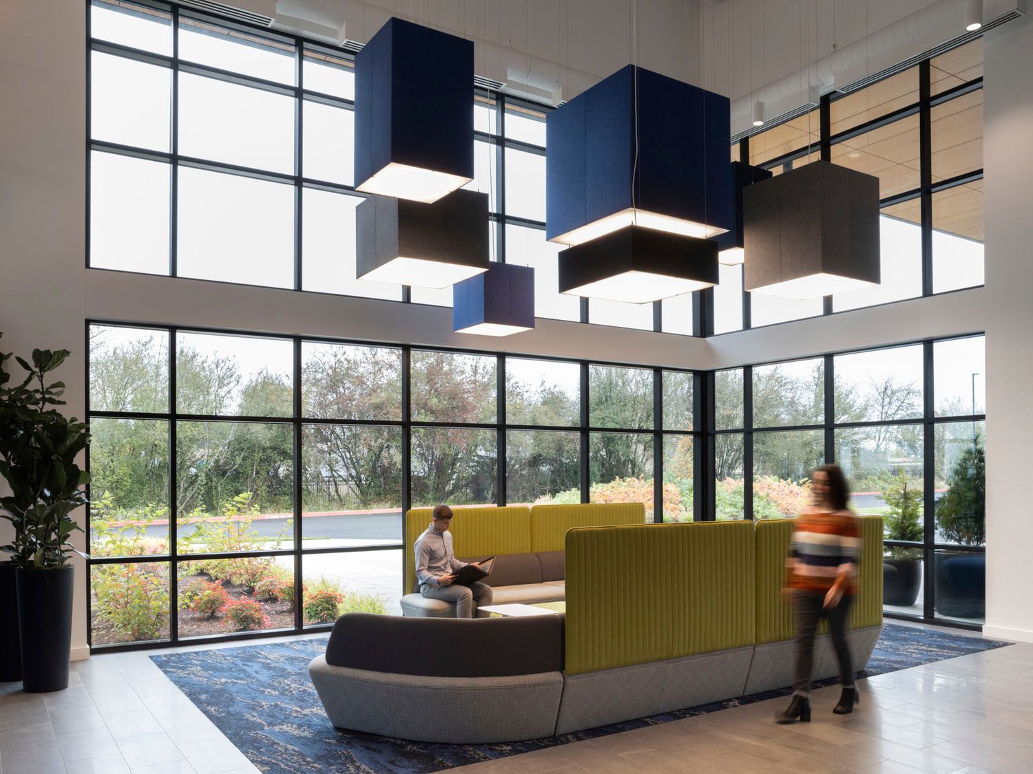
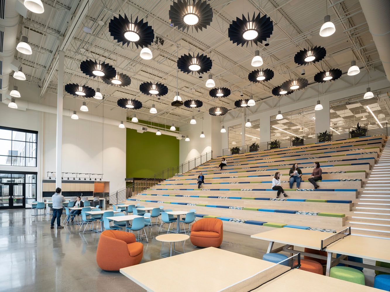
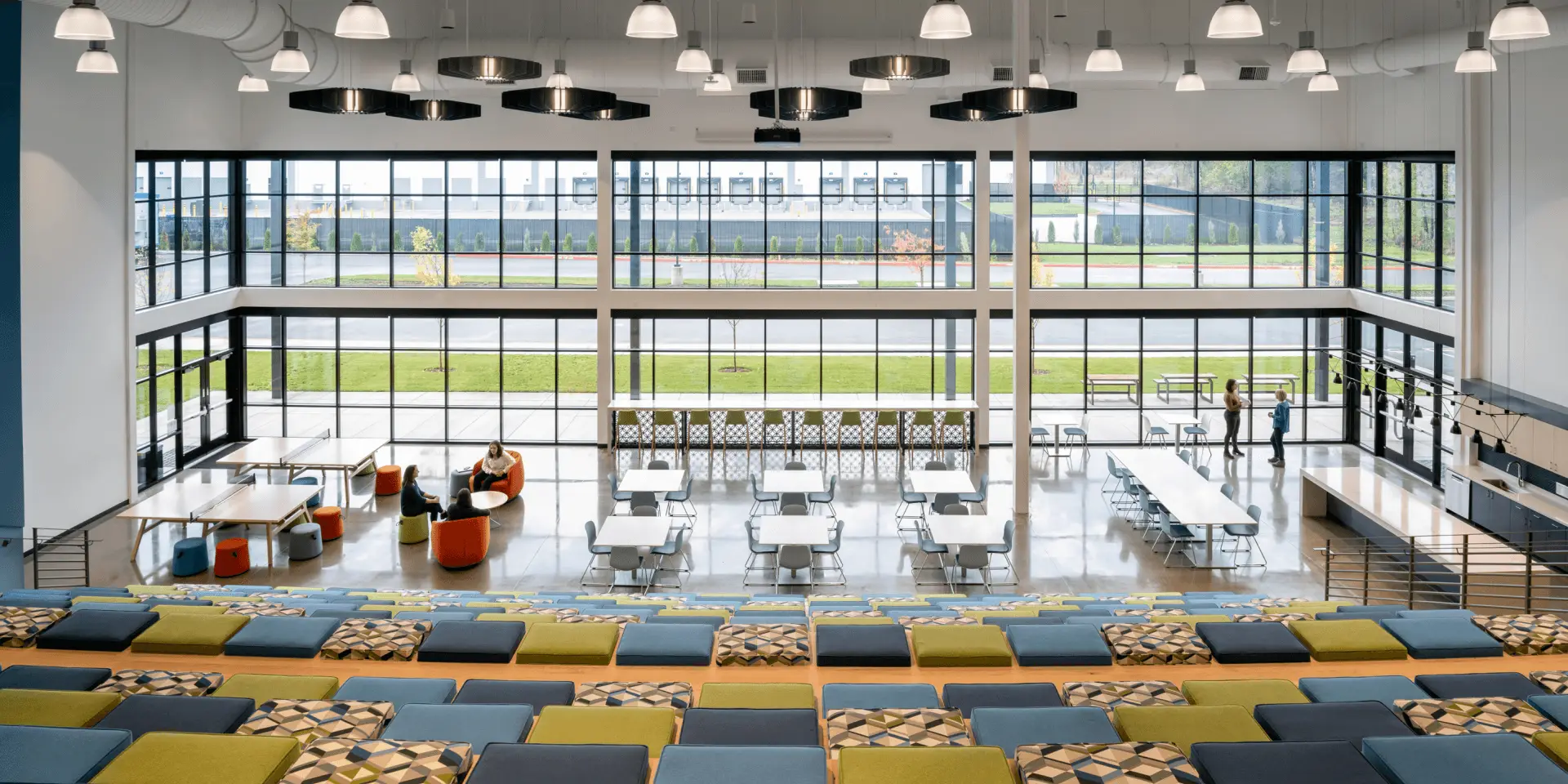
Connection is a cornerstone for this company, and there was a requirement for flexible space for staff to relax or host events. Based on that goal, the team designed a spacious break room and presentation area that capitalized on amazing views.